Title: New addition to the collection.
Post by: SlateBlue on January 18, 2017, 12:40:20 AM
Post by: SlateBlue on January 18, 2017, 12:40:20 AM
I received a color slab today; it made the trek to Kansas all the way from Alaska. According to the gentleman I purchased it from, it was used by a professor at the University of Alaska - Fairbanks, and then eventually made its way to Anchorage. In addition to the slab, I got the 17" monitor, sound box, printer, start-up kit, CD-ROM, fax modem - all in their respective original boxes. I'm still waiting for the software and other documentation to arrive; they were shipped media mail and won't be here until next week.
This thing looks like it was hardly used. I mean, it's in nearly mint condition. The fax modem appears unused. It has 20 MB of RAM and came with a 406 MB hard drive, but I've since removed the hard drive and replaced it with a SCSI2SD. The drive ran insanely hot anyway. I'll post some pics when I get time.
Correct me if I'm wrong: I thought the color slab maxed out at 32 MB of RAM, but I read somewhere that you could upgrade it to 128 MB with 16 MB SIMMs. Is this accurate?
Title: New addition to the collection.
Post by: barcher174 on January 18, 2017, 01:44:19 AM
Post by: barcher174 on January 18, 2017, 01:44:19 AM
If you have 4 RAM slots then yes you're in luck. Otherwise if you have 8 then 32mb is as high as you can go.
Title: New addition to the collection.
Post by: SlateBlue on January 18, 2017, 01:48:30 AM
Post by: SlateBlue on January 18, 2017, 01:48:30 AM
8 slots, so 32 MB it is. Thanks for the clarification.
Title: New addition to the collection.
Post by: SlateBlue on January 19, 2017, 07:17:33 PM
Post by: SlateBlue on January 19, 2017, 07:17:33 PM
I can't find a definitive answer to this question:
Will a non-turbo NeXTstation work with FPM or EDO memory, or both?
Will a non-turbo NeXTstation work with FPM or EDO memory, or both?
Title: New addition to the collection.
Post by: Andreas on January 20, 2017, 01:30:41 AM
Post by: Andreas on January 20, 2017, 01:30:41 AM
Quote from: "SlateBlue"I can't find a definitive answer to this question:
Will a non-turbo NeXTstation work with FPM or EDO memory, or both?
read here in section 5.24:
http://www.museplan.com/projects/next-mac-faq/NeXT-FAQ.txt
the mono you have deals with 30 pin SIMs, a color needs 72 PIN.
The question FPM or EDO came later with the 72 PIN so called "PS2" modules. AFAIK you need FPM, EDO won't work.
Title: New addition to the collection.
Post by: t-rexky on January 20, 2017, 05:01:30 PM
Post by: t-rexky on January 20, 2017, 05:01:30 PM
On a somewhat related note, EDO modules in my Turbo Color work just fine...
Title: New addition to the collection.
Post by: SlateBlue on January 23, 2017, 07:28:38 PM
Post by: SlateBlue on January 23, 2017, 07:28:38 PM
I found a couple of SIMMs to bring my memory total to 26 MB of RAM. I'm waiting on two more sticks to arrive to max it out. Has anyone else attempted to browse this board from his or her NeXT hardware? (I'm typing this entire post from the NeXtstation...) Geez... it's slow. ;)
I'm getting ready to upload a few photos of the machine (from my more modern computer!). In advance, I ask that you pardon the mess and poor lighting. The boxes for the slab and monitor have already been put in storage since I don't have enough room here to put them. The original CD-ROM, printer, and Starting Point kit are downstairs in my living room, still boxed. Since the original keyboard and mouse are in near mint condition, I decided not to use them. @Rob Blessin, do you have replacement pickup and feed rollers for the printers? It doesn't appear that this system had much use, but I'm sure the rollers have deteriorated some after 24 years. The best I can tell, this system was purchased sometime in 1992. I'm still waiting on the software to arrive. I know there are titles such as Mathematica, Create, Adobe Illustrator, Parabase/Sybase SQL, WordPerfect, Improv, and "The Big Green CD." I don't think this list is all inclusive.
Anyway, I've got it set up with the SCSI2SD, and a ~2 GB boot disk with NS 3.3. It had 3.2 installed on the original 400 MB hard disk. When I installed the SCSI2SD, I notice the original hard drive was insanely hot when I removed it. Is it normal for these older SCSI drives to run that hot? The drive wasn't excessively noisy.
Title: New addition to the collection.
Post by: t-rexky on January 23, 2017, 09:09:11 PM
Post by: t-rexky on January 23, 2017, 09:09:11 PM
Quote from: "SlateBlue"[...]I notice the original hard drive was insanely hot when I removed it. Is it normal for these older SCSI drives to run that hot? The drive wasn't excessively noisy.
In my experience, the enterprise Quantum drives from that era run hot enough to burn your hand if you touched them for too long. Others would be similar. It's amazing that some of those drives run for 15+ years!
Title: New addition to the collection.
Post by: SlateBlue on January 23, 2017, 11:01:51 PM
Post by: SlateBlue on January 23, 2017, 11:01:51 PM
Image handling between Google Drive and this board doesn't seem to work as intended. I'll post a link here to the album if anyone wants to see any of the photos I've uploaded. Nothing insanely impressive at this point, but more will be added in the future.
Album Link (https://drive.google.com/open?id=0B5_1dpWRUKulQm54MEYtRUxWaG8)
Album Link (https://drive.google.com/open?id=0B5_1dpWRUKulQm54MEYtRUxWaG8)
Title: New addition to the collection.
Post by: SlateBlue on January 23, 2017, 11:03:25 PM
Post by: SlateBlue on January 23, 2017, 11:03:25 PM
Quote from: "t-rexky"In my experience, the enterprise Quantum drives from that era run hot enough to burn your hand if you touched them for too long. Others would be similar. It's amazing that some of those drives run for 15+ years!
As was the case here. That excessive heat can't be good for everything else inside the computer.
Title: New addition to the collection.
Post by: SlateBlue on February 06, 2017, 03:19:12 PM
Post by: SlateBlue on February 06, 2017, 03:19:12 PM
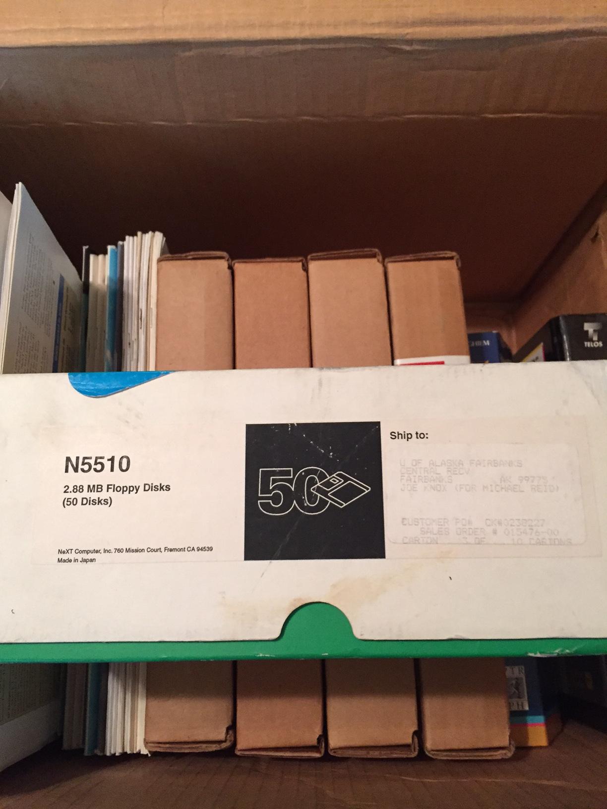
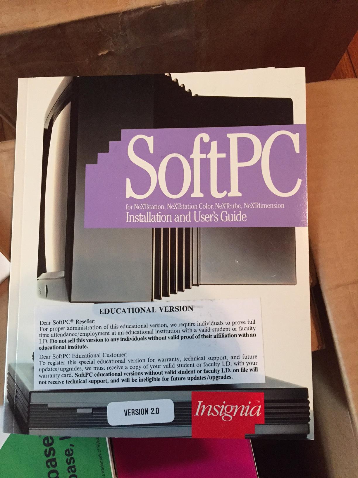
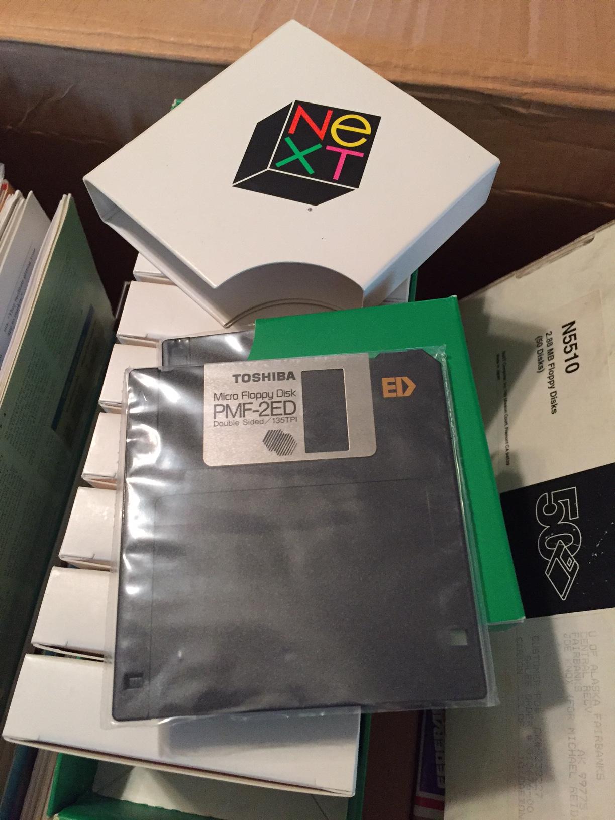
Software and literature arrive today. Photos of some of the included materials (saved the best for last):


Title: New addition to the collection.
Post by: Andreas on February 07, 2017, 12:59:09 AM
Post by: Andreas on February 07, 2017, 12:59:09 AM
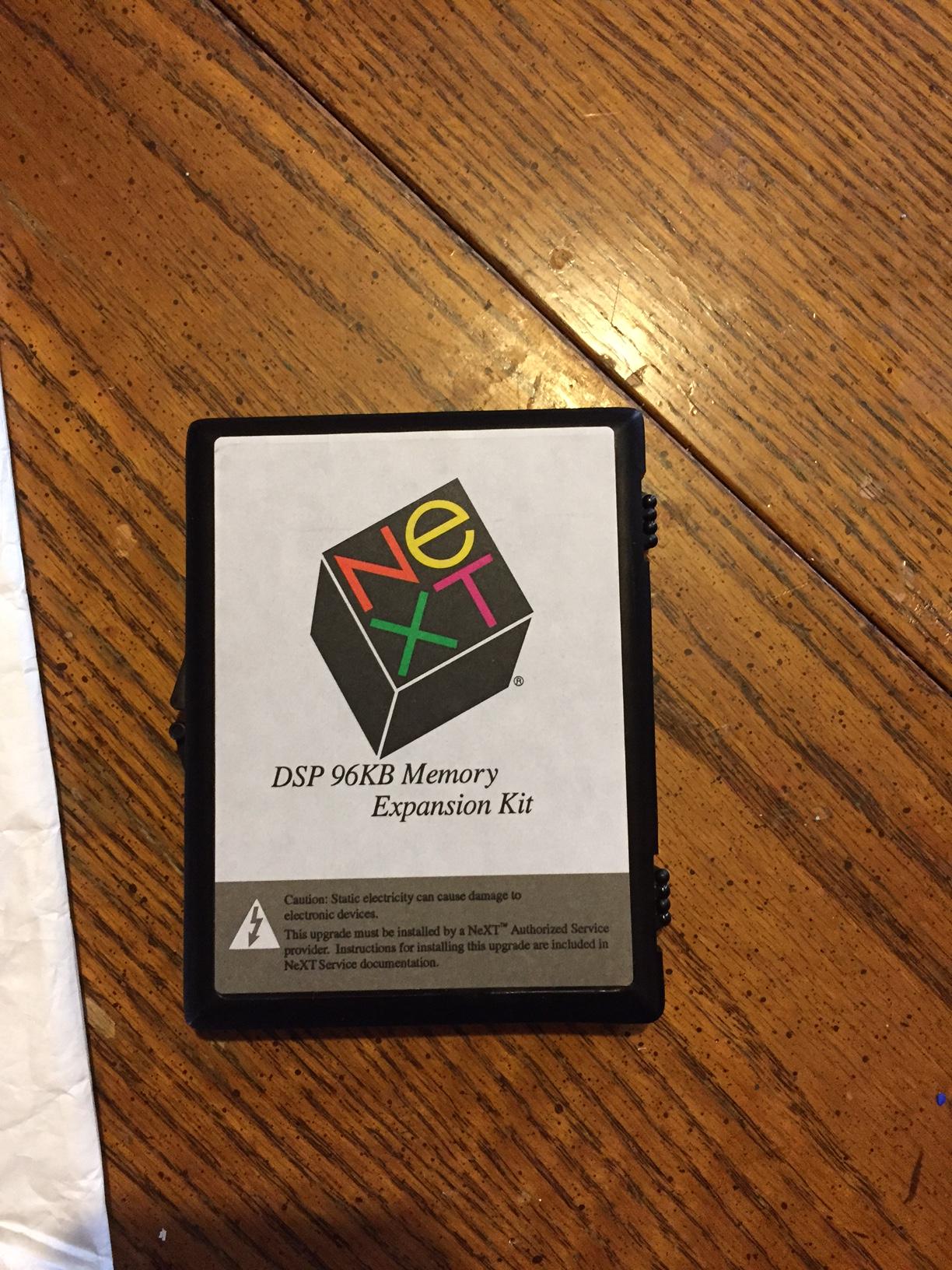
Wow, thats a really good starting point for collecting NeXT stuff. Besides the rare GEM DSP module i would never use that floppys and let the 50 pieces box untouched as collectors item :-)
Title: New addition to the collection.
Post by: SlateBlue on February 07, 2017, 07:09:40 AM
Post by: SlateBlue on February 07, 2017, 07:09:40 AM
I wasn't expecting the floppies or DSP module since they were never mentioned. I knew I was getting literature and software. I literally have three boxes of NeXT/Unix books. I'm with you about not using the floppies. I have no intention of doing so. If I need to use ED disks, I have other non NeXT branded disks available.
Title: New addition to the collection.
Post by: Rob Blessin Black Hole on February 07, 2017, 05:07:01 PM
Post by: Rob Blessin Black Hole on February 07, 2017, 05:07:01 PM
Wow cool DSP module ! I Haagen new old stock NeXT laser printer intake rollers for $15 Best regards Rob
Title: New addition to the collection.
Post by: SlateBlue on February 07, 2017, 07:22:58 PM
Post by: SlateBlue on February 07, 2017, 07:22:58 PM
Thanks, Rob. Have those rollers held up well over the years? Seems I read somewhere that the rubber has a tendency to deteriorate with age.
Title: New addition to the collection.
Post by: Rob Blessin Black Hole on February 07, 2017, 10:40:17 PM
Post by: Rob Blessin Black Hole on February 07, 2017, 10:40:17 PM
Quote from: "SlateBlue"Thanks, Rob. Have those rollers held up well over the years? Seems I read somewhere that the rubber has a tendency to deteriorate with age.ive kept them stored in heated storage ,its the best I can do !
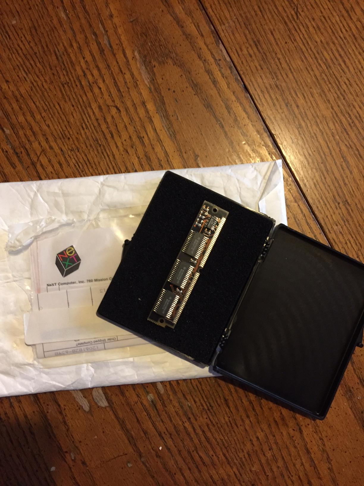
Title: DSP memory
Post by: cubist on February 09, 2017, 10:55:24 PM
Post by: cubist on February 09, 2017, 10:55:24 PM
Would love to get some better front and back images of the DSP memory. Say from a scanner...
Title: New addition to the collection.
Post by: SlateBlue on April 13, 2017, 11:09:21 AM
Post by: SlateBlue on April 13, 2017, 11:09:21 AM
I've been trying to figure out how I can get the DSP module x-rayed so that the community can reproduce it. My brother-in-law is a vet, but he won't waste his time and resources on this hobby. You guys have any other ideas? I'm guessing there is a lack of schematics, otherwise this chip could be recreated?
Title: Re: DSP memory
Post by: pentium on April 13, 2017, 08:36:39 PM
Post by: pentium on April 13, 2017, 08:36:39 PM
Quote from: "cubist"Would love to get some better front and back images of the DSP memory. Say from a scanner...
I photo enhanced a photo from the DSP project a number of years ago
The rest of my efforts are stored here. (http://s11.photobucket.com/user/ballsandy/library/Computer%20related/NeXT%20DSP?sort=3&page=1)
Title: New addition to the collection.
Post by: SlateBlue on April 13, 2017, 09:25:03 PM
Post by: SlateBlue on April 13, 2017, 09:25:03 PM
I'm no electronics guru, but since I have a physical module, wouldn't I be able to tone out all the connections with a multimeter? I assume it would be cumbersome, but doable.
Title: New addition to the collection.
Post by: bobo68 on April 14, 2017, 08:36:35 AM
Post by: bobo68 on April 14, 2017, 08:36:35 AM
You probably could. Use the connectivity check function and try to avoid sending current through the chips. There is starting material here: http://www.nextcomputers.org/NeXTfiles/Projects/DSP_Expansion_Ram/
I used this http://www.nextcomputers.org/NeXTfiles/Projects/DSP_Expansion_Ram/SFSU_NeXT_DSP_Expansion_Memory.pdf (this design is for a larger DSP memory - 256 K x 8 ) as a basis.
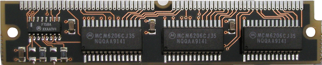
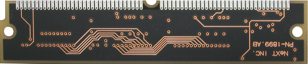
It's always good to work based on a hypothesis and deduct as much as possible just from the traces. Here is what I see:
The design should be straight forward. The pins of the SIMM module are counted from the indent from 1 to 64. 1 to 36 are the 24 data lines from the bus with Vcc supply lines and ground lines in between. The SRAM chips are 8 bit wide so their data lines are directly mapped across the bus data lines (i.e. the lowest data lines to the chip on the left, the next one's the one in the middle, ...).
37 - 56 are the 16 address lines of the bus again with Vcc and ground lines in between. The 14 lowest should go directly to the 14 address lines of the SRAMs.
The highest lines starting with 57 are interesting and they will probably go together with the other logic chip (a 4 line 2 input multiplexer).
57 - DSPXY - an additional address line?! - we do not need it
58 - DSPRD - signals a read - goes to output enable of the SRAMs
59 - DSPWR - signals a write - goes to write enable of the SRAMs
60 - DSPRMEM - chip enable - goes to chip enable of the SRAMs
62 - DSPPS - chip enable - dito?!
63 - SRAMCS - some chip select - following the traces it seems to go to chip enable of the middle SRAM and somewhere else (it splits)
58, 59 and 60 might be inverted before going to the SRAMs.
I used this http://www.nextcomputers.org/NeXTfiles/Projects/DSP_Expansion_Ram/SFSU_NeXT_DSP_Expansion_Memory.pdf (this design is for a larger DSP memory - 256 K x 8 ) as a basis.
It's always good to work based on a hypothesis and deduct as much as possible just from the traces. Here is what I see:
The design should be straight forward. The pins of the SIMM module are counted from the indent from 1 to 64. 1 to 36 are the 24 data lines from the bus with Vcc supply lines and ground lines in between. The SRAM chips are 8 bit wide so their data lines are directly mapped across the bus data lines (i.e. the lowest data lines to the chip on the left, the next one's the one in the middle, ...).
37 - 56 are the 16 address lines of the bus again with Vcc and ground lines in between. The 14 lowest should go directly to the 14 address lines of the SRAMs.
The highest lines starting with 57 are interesting and they will probably go together with the other logic chip (a 4 line 2 input multiplexer).
57 - DSPXY - an additional address line?! - we do not need it
58 - DSPRD - signals a read - goes to output enable of the SRAMs
59 - DSPWR - signals a write - goes to write enable of the SRAMs
60 - DSPRMEM - chip enable - goes to chip enable of the SRAMs
62 - DSPPS - chip enable - dito?!
63 - SRAMCS - some chip select - following the traces it seems to go to chip enable of the middle SRAM and somewhere else (it splits)
58, 59 and 60 might be inverted before going to the SRAMs.
Title: New addition to the collection.
Post by: SlateBlue on April 14, 2017, 03:18:47 PM
Post by: SlateBlue on April 14, 2017, 03:18:47 PM
You're saying that putting current through a chip by way of a continuity test may damage the chip? I'm not sure how I would avoid this. I don't want to risk damaging the module.
Title: New addition to the collection.
Post by: bobo68 on April 14, 2017, 03:31:07 PM
Post by: bobo68 on April 14, 2017, 03:31:07 PM
Yes, the test current or voltage may harm chips.
Work your way forward step by step from the SIMM's 64 contacts and do not measure across chips, i.e. do not put the multimeter's leads on two pins of a chip.
Work your way forward step by step from the SIMM's 64 contacts and do not measure across chips, i.e. do not put the multimeter's leads on two pins of a chip.
Title: New addition to the collection.
Post by: bobo68 on April 14, 2017, 04:05:28 PM
Post by: bobo68 on April 14, 2017, 04:05:28 PM
I went a bit through some info on the DSP56001:
http://www.nxp.com/assets/documents/data/en/data-sheets/DSP56001.pdf
http://simson.net/ref/NeXT/byte/dsp.htm
http://uploads.cq-dx.ru/pdf/DSP/DSP56001UM2.PDF (uuuh Russia...)
http://cache.freescale.com/files/dsp/doc/inactive/DSP56001A.pdf
It seems to me that the DSP needs so called X and Y data memory to be present and maybe also program memory. So the DSPXY line would be used and DSPPS / DS as well.
As I said it would be good to find out how the pins 57 to 64 are wired.
Title: New addition to the collection.
Post by: SlateBlue on April 14, 2017, 09:32:48 PM
Post by: SlateBlue on April 14, 2017, 09:32:48 PM
When I get some time, I'll read through that documentation and see if I can add anything useful.
Title: New addition to the collection.
Post by: bobo68 on April 15, 2017, 07:02:39 AM
Post by: bobo68 on April 15, 2017, 07:02:39 AM
You will not get much information from these docs for the task of understanding the wiring diagram of the SIMMs module. We could start with a Google spreadsheet in which we work on the SIMMs wiring.
BTW, sometimes you can see through the module if you hold it up to a strong light source. If the module has a complete Vcc or ground plane than you would not see much, though.
BTW, sometimes you can see through the module if you hold it up to a strong light source. If the module has a complete Vcc or ground plane than you would not see much, though.
Title: New addition to the collection.
Post by: SlateBlue on April 15, 2017, 02:53:06 PM
Post by: SlateBlue on April 15, 2017, 02:53:06 PM
I took several photos of the module with it held near a fluorescent lamp. I'm guessing this module is composed of at least four layers? Anyway: link to Imgur album (http://imgur.com/a/5UDHC). You're correct, bobo68, there isn't much to be seen.
Title: New addition to the collection.
Post by: bobo68 on April 15, 2017, 03:05:01 PM
Post by: bobo68 on April 15, 2017, 03:05:01 PM
I guess it is 4 layers because there is a nearly continuous ground (or Vcc?) layer and then at least one internal layer for traces. More layers would be unusual for such a simple thing as a RAM module.
Ok, how shall we proceed?
Ok, how shall we proceed?
Title: New addition to the collection.
Post by: SlateBlue on April 15, 2017, 03:18:34 PM
Post by: SlateBlue on April 15, 2017, 03:18:34 PM
I'm probably going to need some guidance here. I have downloaded the documentation for the F158 mux in order to see the pinout. Do you have documentation of the memory chips? It may or may not help me understand how some of this goes together. If you want to create a spreadsheet and share it with me (Google Docs?) I can fill in what the continuity test tells me. This board has many vias, those vias appear to connect to some internal traces and I can't see where they go. It would appear to me that the ground plane exists on the side opposite of where the components are mounted. So, I then assume the Vcc plane exists on the component side. Thus, ground pins would be on the backside of the module, and Vcc pins would be on the front. Is this correct?
Again, I am no electronics guru, but I can learn. So, if my questions are a bit elementary, be patient as I'm just simply trying to grasp understanding.
Again, I am no electronics guru, but I can learn. So, if my questions are a bit elementary, be patient as I'm just simply trying to grasp understanding.
Title: New addition to the collection.
Post by: SlateBlue on April 15, 2017, 03:49:13 PM
Post by: SlateBlue on April 15, 2017, 03:49:13 PM
Documents for both the F158 mux and memory chips: here (https://drive.google.com/drive/folders/0B5_1dpWRUKulcHFHdk0wZFFHMEk?usp=sharing).
Title: New addition to the collection.
Post by: SlateBlue on April 15, 2017, 08:08:36 PM
Post by: SlateBlue on April 15, 2017, 08:08:36 PM
I've created a spreadsheet and have documented what I've toned out so far. The way I have it laid out makes sense to me, although I have not tried to discern any kind of pattern. It would appear to me, through visual inspection, that some of the pins on each memory chip are connected in parallel. Does this make sense?
Link To Spreadsheet (https://docs.google.com/spreadsheets/d/1IEQZNNyqNDBm2rji7DHeYrpfK_TktUw3WzUsdI8wsJM/edit?usp=sharing)
I'm going to take a break and go watch Lifetime movies with my wife. ;)
Link To Spreadsheet (https://docs.google.com/spreadsheets/d/1IEQZNNyqNDBm2rji7DHeYrpfK_TktUw3WzUsdI8wsJM/edit?usp=sharing)
I'm going to take a break and go watch Lifetime movies with my wife. ;)
Title: New addition to the collection.
Post by: bobo68 on April 16, 2017, 05:22:58 AM
Post by: bobo68 on April 16, 2017, 05:22:58 AM
I'll have a look at the spreadsheet. Of course that makes sense, (most of) the address lines would be connected to all address inputs of the RAM chips. Same for read/write signal lines.
Title: New addition to the collection.
Post by: bobo68 on April 16, 2017, 08:17:08 AM
Post by: bobo68 on April 16, 2017, 08:17:08 AM
Quote from: "SlateBlue"This board has many vias, those vias appear to connect to some internal traces and I can't see where they go. It would appear to me that the ground plane exists on the side opposite of where the components are mounted. So, I then assume the Vcc plane exists on the component side. Thus, ground pins would be on the backside of the module, and Vcc pins would be on the front. Is this correct?
Most probably not. I do not know if there is really one ground and additionally one Vcc layer (plane). It could just be a ground layer and direct connections (via distinct traces) for Vcc.
A via can go to any other layer, either an internal one or through to the other outer layer.
I do not know what you mean with the ground pins on the backside etc. The pins of the SIMM module do not have two separate sides, they are connected.
In your spreadsheet we will need to document inter-component connections, too.
Title: New addition to the collection.
Post by: bobo68 on April 16, 2017, 08:44:09 AM
Post by: bobo68 on April 16, 2017, 08:44:09 AM
Here is the DSP expansion slot as documented in the 33MHz NeXT Color Slab Motherboard Schematics: http://www.nextcomputers.org/NeXTfiles/Docs/Hardware/Schematics/Turbo_slab/CSlab33-09.pdf
It says that pin 42 of the SIMM is _DSPDS which is (inverted) data select. Interesting to see that the guys who build the large DSP memory module did not use the pin but inverted _DSPPS to get _DSPDS. From the 56001 documentation these seem to be mutually exclusive (either program memory or data memory and data memory could be x memory or y memory signaled by DSPXY).
There is some other interesting information here https://heller.userweb.mwn.de/NeXT/HW_internal_FAQ.txt
Sounds like NeXT used some kind of memory overlay scheme ("image"?) to me. We will find out when we understand the wiring of the multiplexer.
It says that pin 42 of the SIMM is _DSPDS which is (inverted) data select. Interesting to see that the guys who build the large DSP memory module did not use the pin but inverted _DSPPS to get _DSPDS. From the 56001 documentation these seem to be mutually exclusive (either program memory or data memory and data memory could be x memory or y memory signaled by DSPXY).
There is some other interesting information here https://heller.userweb.mwn.de/NeXT/HW_internal_FAQ.txt
Code Select
Subject: L10. How to expand DSP memory?

The Speech Recognition Lab at San Francisco State University has
developed a DSP memory expansion board for the NeXT computer that
provides the maximum memory supported by the DSP56001 processor.

...

Note: Because we've organized our memory as three separate
(non-overlapping) banks (X, Y and P) of 192KB apiece, none of the DSP
memory image functionality provided by NeXT with its existing 8K base
configuration, or its 96KB DSP expansion module is supported. While we
cannot guarantee that every existing DSP application ever written will
be plug-and-play compatable with our DSP expansion memory, we are not
aware of any existing applications that use the image functionality.
The MusicKit, and demo programs that use the DSP, such as Mandlebrot
and ScorePlayer, work fine with our memory module.
Sounds like NeXT used some kind of memory overlay scheme ("image"?) to me. We will find out when we understand the wiring of the multiplexer.
Title: New addition to the collection.
Post by: SlateBlue on April 16, 2017, 11:04:46 AM
Post by: SlateBlue on April 16, 2017, 11:04:46 AM
Quote from: "bobo68"Yes, disregard. I forgot this was a SIMM when I made that comment.Quote from: "SlateBlue"This board has many vias, those vias appear to connect to some internal traces and I can't see where they go. It would appear to me that the ground plane exists on the side opposite of where the components are mounted. So, I then assume the Vcc plane exists on the component side. Thus, ground pins would be on the backside of the module, and Vcc pins would be on the front. Is this correct?
Most probably not. I do not know if there is really one ground and additionally one Vcc layer (plane). It could just be a ground layer and direct connections (via distinct traces) for Vcc.
A via can go to any other layer, either an internal one or through to the other outer layer.
I do not know what you mean with the ground pins on the backside etc. The pins of the SIMM module do not have two separate sides, they are connected.
In your spreadsheet we will need to document inter-component connections, too.
Title: New addition to the collection.
Post by: SlateBlue on April 16, 2017, 11:29:52 AM
Post by: SlateBlue on April 16, 2017, 11:29:52 AM
Quote from: "bobo68"In your spreadsheet we will need to document inter-component connections, too.Agreed. I figured I would start by figuring out where each pin on the SIMM connects to. I am going now to have Easter lunch with some friends and will return this afternoon.
Title: New addition to the collection.
Post by: bobo68 on April 16, 2017, 02:10:04 PM
Post by: bobo68 on April 16, 2017, 02:10:04 PM
Quote from: "bobo68"Sounds like NeXT used some kind of memory overlay scheme ("image"?) to me. We will find out when we understand the wiring of the multiplexer.
According to the DSP56001 24-BIT DIGITAL SIGNAL PROCESSOR USER'S MANUAL an overlay scheme should not be present:
Code Select
The program memory select, data memory select, and X/Y select can be considered additional address signals, which extend the addressable memory from 64K words to 192K wordsBut who knows what NeXT made out of it.
Title: New addition to the collection.
Post by: SlateBlue on April 16, 2017, 03:31:26 PM
Post by: SlateBlue on April 16, 2017, 03:31:26 PM
Quote from: "bobo68"Here is the DSP expansion slot as documented in the 33MHz NeXT Color Slab Motherboard Schematics: http://www.nextcomputers.org/NeXTfiles/Docs/Hardware/Schematics/Turbo_slab/CSlab33-09.pdfWhat is meant by memory overlay? Does this refer to how the memory is managed?
It says that pin 42 of the SIMM is _DSPDS which is (inverted) data select. Interesting to see that the guys who build the large DSP memory module did not use the pin but inverted _DSPPS to get _DSPDS. From the 56001 documentation these seem to be mutually exclusive (either program memory or data memory and data memory could be x memory or y memory signaled by DSPXY).
There is some other interesting information here https://heller.userweb.mwn.de/NeXT/HW_internal_FAQ.txtCode SelectSubject: L10. How to expand DSP memory?
The Speech Recognition Lab at San Francisco State University has
developed a DSP memory expansion board for the NeXT computer that
provides the maximum memory supported by the DSP56001 processor.
...
Note: Because we've organized our memory as three separate
(non-overlapping) banks (X, Y and P) of 192KB apiece, none of the DSP
memory image functionality provided by NeXT with its existing 8K base
configuration, or its 96KB DSP expansion module is supported. While we
cannot guarantee that every existing DSP application ever written will
be plug-and-play compatable with our DSP expansion memory, we are not
aware of any existing applications that use the image functionality.
The MusicKit, and demo programs that use the DSP, such as Mandlebrot
and ScorePlayer, work fine with our memory module.
Sounds like NeXT used some kind of memory overlay scheme ("image"?) to me. We will find out when we understand the wiring of the multiplexer.
Title: New addition to the collection.
Post by: bobo68 on April 17, 2017, 05:24:37 AM
Post by: bobo68 on April 17, 2017, 05:24:37 AM
Overlay means in this case that the logical memory space (as addressed by the bus) is mapped to the physical memory (as provided by the SRAMs) in such a manner that more than one logical address spaces is mapped to the same physical address space.
I introduced an address mapping table in the Google sheet which shows my current understanding.
It is done by the multiplexer, which uses the DSPA15 bus signal to either provide bus DSPA14 or bus DSPXY line (inverted) to A14 of the SRAM. By that the 192 K word address space (64 K of program, data x and data y memory) is mapped to 32 K SRAM address space in some weird manner.
Title: New addition to the collection.
Post by: SlateBlue on April 17, 2017, 10:12:16 AM
Post by: SlateBlue on April 17, 2017, 10:12:16 AM
I have added comments where original notes were ambiguous. It appears _DSPDS is still in question, so I will work to see if there is any correlation with pin 42 of the SIMM.